SPI screen parameter configuration
Interface description
In software, SPI interfaces are first divided into two major categories according to whether the SPI interface has a physical D/CX line: LCDC_INTF_SPI_DCX_xxx and LCDC_INTF_SPI_NODCX_xxx. They are then divided into 1~4DATA according to the number of data lines used when sending data in bulk (that is, the 0x2C/0x3C commands). Finally, DDR and AUX are added according to whether DDR is used and whether PTC assistance is required.
Generally, 3-line SPI means there is no physical D/CX line, while 4-line SPI has a physical D/CX line.
The pinmux of the D/CX line is usually LCDC_SPI_DIO1.
SPI interface command reads and writes are all in single-line mode. Only when sending data in bulk (0x2c/0x3c commands) can the data support 1~4 lines in parallel.
Interface name |
Whether the interface has a physical D/CX line |
Number of parallel data lines for bulk data transfer by 0x2C/0X3C |
Other |
|---|---|---|---|
LCDC_INTF_SPI_DCX_1DATA |
Yes |
1 |
- |
LCDC_INTF_SPI_DCX_2DATA |
Yes |
2 |
- |
LCDC_INTF_SPI_DCX_4DATA |
Yes |
4 |
- |
LCDC_INTF_SPI_DCX_4DATA_AUX |
Yes |
4 |
ramless screen |
LCDC_INTF_SPI_DCX_DDR_4DATA |
Yes |
4 |
DDR mode |
LCDC_INTF_SPI_NODCX_1DATA |
No |
1 |
- |
LCDC_INTF_SPI_NODCX_2DATA |
No |
1 |
- |
LCDC_INTF_SPI_NODCX_4DATA |
No |
1 |
- |
Screen parameter configuration explanation
4-line/3-line SPI interface
static LCDC_InitTypeDef lcdc_int_cfg =
{
/*
    3线SPI模式,批量送数2根数据线
*/
    .lcd_itf = LCDC_INTF_SPI_NODCX_2DATA,
/*  QSPI的clk频率选择,频率为hcpu主频分频后的频率,比如hcpu主频240Mhz,能够得到的频率只能为40/48/60/80,如果设置62Mhz,实际会设置为60Mhz */
    .freq = 24000000,
    .color_mode = LCDC_PIXEL_FORMAT_RGB565,

    .cfg = {
        .spi = {
            .dummy_clock = 0, /* Yes在QSPI读模式下,配置cmd和data之间空的clk数量,默认为0,不用修改 */
/* 该选项Yes为了避免出现图像撕裂,(出现撕裂原因:屏读取RAM数据时,QSPI也在往RAM送数) */
#ifdef LCD_ST7789P3_VSYNC_ENABLE
            .syn_mode = HAL_LCDC_SYNC_VER,/* 启动检查屏送出的TE信号,并同步给RAM送数,打开此配置,如果屏无TE信号输出,会出现无法给RAM送数,出现死机 */
#else
			.syn_mode = HAL_LCDC_SYNC_DISABLE,/* 关闭检查屏送出的TE信号,在刚开始调试屏驱动,不考虑撕裂问题时,采用此配置 */
#endif
/*
该配置在选择HAL_LCDC_SYNC_VER后,才有意义,用于配置TE(Vsync)信号来时的信号极性,
配置为1,TE平常Yes低电平,TE为高电平时可以给RAM送数
*/
            .vsyn_polarity = 0,
            .vsyn_delay_us = 1000,/* 该配置在选择HAL_LCDC_SYNC_VER后,才有意义,用于配置TE信号高电平延时多少us后,再给RAM送数*/
            .hsyn_num = 0,/* 该配置在.syn_mode设置为HAL_LCDC_SYNC_VERHOR后才有意义,用于配置TE信号高电平几个clk脉冲后,再给RAM送数 */
/*
1. 在QSPI读数据的时候,CMD都会从D0输出,但Yes读回的数据,不同屏驱IC,会从D0-D3进行输出,为了兼容不同的屏驱IC,才有此配置
2. 可以配置为0-3,参考屏驱IC的规格书,选择QSPI对应read时从D0 - D3进行读取信号
*/
            .readback_from_Dx = 0,
        },
    },
};
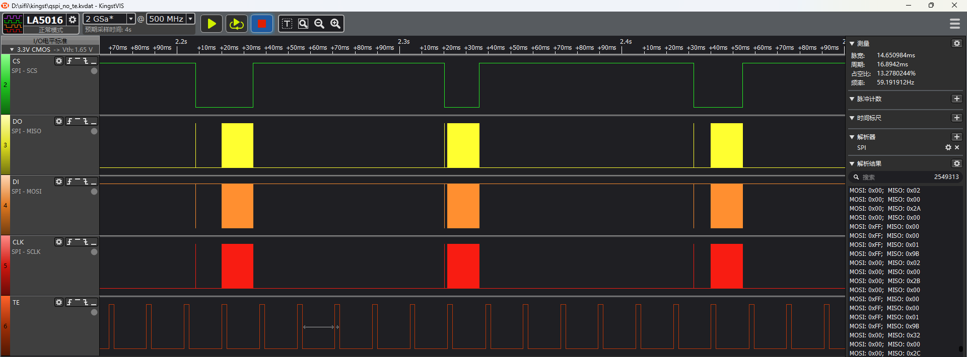
The following figure shows the waveform when Yes 4-line TE is not enabled. You can see that the TE waveform is not aligned with the falling edge of SPI CS.
Frame rate test method
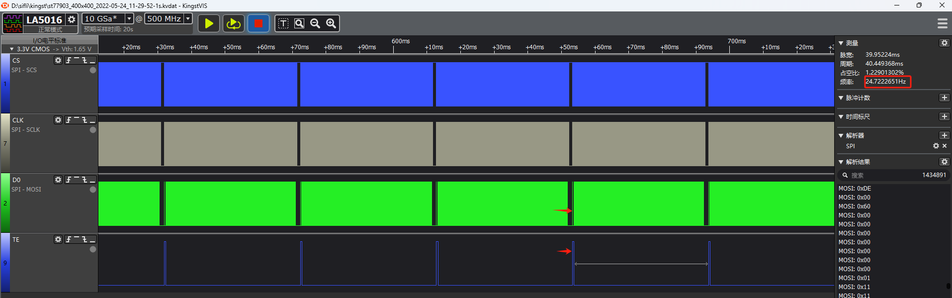
Enable the HAL_LCDC_SYNC_VER configuration. The SPI timing is shown below, and screen data transfer will be aligned with TE
On a UI screen with a very high frame rate, check the frequency of the test TE; it should reach the screen refresh frame rate
QSPI interface
#ifdef LCDC_USE_DDR_QSPI
    #define QAD_SPI_ITF LCDC_INTF_SPI_DCX_DDR_4DATA
    #define QAD_SPI_ITF_FREQ   40000000
#else
    #define QAD_SPI_ITF LCDC_INTF_SPI_DCX_4DATA
    #define QAD_SPI_ITF_FREQ   48000000
#endif
static LCDC_InitTypeDef lcdc_int_cfg_spi =
{
 /*
 1. DDR(qspi的clk双沿送数方式)选择 LCDC_INTF_SPI_DCX_DDR_4DATA
2. SDR(qspi的clk单沿送数方式)选择 LCDC_INTF_SPI_DCX_4DATA
 */
    .lcd_itf = QAD_SPI_ITF, //LCDC_INTF_SPI_NODCX_1DATA,
/*
1. QSPI的clk频率选择,频率为hcpu主频分频后的频率,比如hcpu主频240Mhz,能够得到的频率只能为40/48/60/80,如果设置62Mhz,实际会设置为60Mhz
2. DDR mode下,QSPI的clk频率不能设置过高
*/
    .freq = QAD_SPI_ITF_FREQ,
/*
1. LCDC_PIXEL_FORMAT_RGB565为常见的RGB565色
2. LCDC_PIXEL_FORMAT_RGB888为常见的RGB888色
*/
#if LV_COLOR_DEPTH == 24
    .color_mode = LCDC_PIXEL_FORMAT_RGB888,
#else
    .color_mode = LCDC_PIXEL_FORMAT_RGB565,
#endif

    .cfg = {
        .spi = {
            .dummy_clock = 0, /* Yes在QSPI读模式下,配置cmd和data之间空的clk数量,默认为0,不用修改 */
/* 该选项Yes为了避免出现图像撕裂,(出现撕裂原因:屏读取RAM数据时,QSPI也在往RAM送数)*/
#ifdef LCD_FT2308_VSYNC_ENABLE
            .syn_mode = HAL_LCDC_SYNC_VER, /* 启动检查屏送出的TE信号,并同步给RAM送数,打开此配置,如果屏无TE信号输出,会出现无法给RAM送数,出现死机*/
#else
            .syn_mode = HAL_LCDC_SYNC_DISABLE, /* 关闭检查屏送出的TE信号,在刚开始调试屏驱动,不考虑撕裂问题时,采用此配置 */
#endif
/* 该配置在选择HAL_LCDC_SYNC_VER后,才有意义,用于配置TE(Vsync)信号来时的信号极性 */
            .vsyn_polarity = 1, /*  配置1,TE平常Yes低电平,TE为高电平时可以给RAM送数 */
            .vsyn_delay_us = 0, /* 该配置在选择HAL_LCDC_SYNC_VER后,才有意义,用于配置TE信号高电平延时多少us后,再给RAM送数 */
            .hsyn_num = 0, /* 该配置在.syn_mode设置为HAL_LCDC_SYNC_VERHOR后才有意义,用于配置TE信号高电平几个clk脉冲后,再给RAM送数 */
 /*
 1. 在QSPI读数据的时候,CMD都会从D0输出,但Yes读回的数据,不同屏驱IC,会从D0-D3进行输出,为了兼容不同的屏驱IC,才有此配置
2. 可以配置为0-3,参考屏驱IC的规格书,选择QSPI对应read时从D0 - D3进行读取信号
 */
            .readback_from_Dx= 3,       /*!< 0 read back data from D0 (HW SPI support), 1 read back from D1(Software SPI support).*/
#ifdef LCDC_USE_DDR_QSPI
            .flags = SPI_LCD_FLAG_DDR_DUMMY_CLOCK,/* 该标志位Yes为了适配DDR屏,DDR mode下送完framebuffer后加入几个空clock */
#endif /* LCDC_USE_DDR_QSPI */
        },
    },

};